Physical Principle of Functioning Molecular Electronic Devices Based on Structural Instability of Low-Dimensional Molecular System
Institute of Inorganic Chemistry, Novosibirsk, Russia
This is an abstract
for a presentation given at the
Sixth
Foresight Conference on Molecular Nanotechnology.
There will be a link from here to the full article when it is
available on the web.
Introduction
One of the reasons for forming and developing molecular electronics is connected with increasing problems in the further development of traditional semiconductor electronics. On the one hand, it is connected with further miniaturization, that is the decreasing of design rules. On the other hand, the physical principle of functioning semiconductor devices are disturbed under less design rules.
Researchers dealing with semiconductor physics and electronics relate the further development of Computer Electronics to using a new physical principle of functioning electronic devices. It is supposed that this physical principle must be based on a quantum phenomenon. So far, many of such phenomena have been suggested and studied. Some of them are the tunnel effect; the Aharonov-Bohm effect; the Coulomb blockade; the physical properties of an artificial low-dimensional structure (two, one and zero dimensional). Many researchers have made and studied a single device whose work is based on such phenomena.
Today, it is clear for all researchers that it is not possible to make many millions of such devices for modern electronic chips. Another direction of solving the problem of modern electronics is the development of molecular electronics. Its goal is creating molecular electronic devices which use the molecular system as an ideal quantum structure. At present we cannot say that a molecular electronic device could function on the level of a single molecule. Now it's practical to talk about the application of intramolecular electron effects which have a macroscopic display and use such a molecular system as new work material. This approach will be called functional molecular electronics. A functional step of the development of molecular electronics is a natural and necessary step of the its development. In all probability this step will take rather longer then now it is expected.
A lot of very interesting investigations have been made in this field recently. However, so far it is not clear what is the best way of using the physical properties of the molecular quantum structure. As in semiconductor electronics, it is necessary to find out the physical principle of functioning new electronic devices (Krieger 1993).
In this paper, I would like to focus attention on the possibility of using the physical phenomena of a low dimensional molecular system for designing new electronic devices (Krieger 1996).
Background
The phenomenon of the electronic-structure instability in a one-dimensional electronic system was theoretically predicted by Peierls in 1955 in his book Quantum Theory of Solids. According to his assumption, a one-dimensional (or low-dimensional) metal with a half-filled band is structurally unstable against the lattice modulation and distortion and opening the dielectric gap leading to the transition of the metal state to a semiconductor or dielectric state (Fig. 1). In other words, a simple one-dimensional lattice, which consists of atoms with one electron per lattice unit and equal distances between the neighboring atoms can be distorted and transformed into a lattice with short and long distances between neighboring atoms. The important characteristics of this phenomenon is the gap value at a zero temperature. The gap value depends on many factors. In particular, one of them is temperature. It leads to the phase transition which is known as Peierls transition. Without going into details, we can obtain for the phase transition temperature the following relation (the gap value is equal 1,76Tp, where Tp is temperature of the phase transition. By now, extensive experimental and theoretical studies of this phenomenon have been carried out. In the first place, these investigation have been connected with problems of superconductivity.
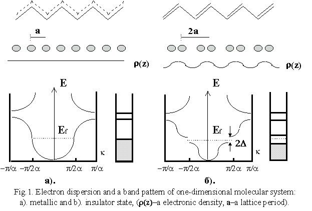
Classical examples of the Peierls systems are polyacetylene and related polyconjugated polymers. Polyacetylene has clearly alternating double and single bonds (Fig. 1). The difference between their lengths is 0.06-0.08 Å. It is known, polyacetylene can be easily transformed from dielectric state to metallic state by doping it with positive or negative ions. Electrical conductivity of the polyacetylene samples can be obtained depending on doping concentration. The doping effect can be explained in different ways. From a chemistry perspective, doping is described as oxidation or reduction reactions, in band theory, as a change in band packing. From a low-dimensional physics perspective, a result of doping is caused by a change in the dimension of electronic systems. In other words, intercalation of the conjugate molecular systems by ions leads to the excitation of one-dimensional electron wave functions, thereby changing the dimension of this system. We believe that such perturbation of an electron system may be induced not only by ion doping, but also by applying an external electrical or magnetic field, electromagnetic radiation, pressure or actions of chemical compounds.
Therein lies our general suggestion for using this phenomenon in Molecular Electronics. From the point of view of molecular electronics, we must be interested in other reasons for changing the gap value and conductivity, respectively (especially with external fields: electrical, magnetic and so on). For this purpose we will analyze factors which define the gap value and observe conditions of the phenomenon of electronic instability in the given system. In other words, we must find ways of controlling the physical properties, especially conductivity, such molecular systems without changing the temperature.
The amplitude of gap depends on a series of factors; from a molecular electronics stand point the most important for us are:
- the change of the charge per lattice period;
- the change of the relative difference of the transfer integrals for the short and long bonds;
- the variation of the transfer integrals between neighboring one-dimensional molecular systems;
- the disorder of the molecular units of one-dimensional systems or guest molecules or ions which are located between neighboring systems.
In order to observe the electron instability, we have to use a one-dimensional molecular system with a value of no less than 50-100 Å. In other words, the dimension of future molecular electronic devices will be about 50 Å and more. From the point of view of Electronics , it is desirable, that this variation should be made by an external electrical field and electrical conductivity could be controlled. When designing devices it is necessary for the state of one dimensional electronic system to be entered into the instability region of the Peierls's quasi-transitions. It can be achieved also by use of the factors listed above.
Basic Ideas of Designing Electronic Devices
To design molecular electronics devices let us consider polyconjugated molecular systems, although it is applicable for other families of one-dimensional systems with different type of organization. These may be organic, organometalic and inorganic compounds. The electronic state of a one-dimensional system can be changed not only with intercalation mechanisms, but also via certain active molecular units, which lie in close vicinity to the van der Waals interaction or chemically bound with one.
To illustrate let us consider design devices, which perform the function of an amplifier (a molecular transistor). There are many ways of designing a molecular transistor. First of all we shall consider ways of changing the charge of a single element in a one-dimensional system. It can be reached at the expense of donor or acceptor molecules connected with an one-dimensional system or located in immediate proximity. In last case, we have the charge transfer system which consists of a polyconjugated molecular system and donor or acceptor molecules. The value of the transferred charge in such systems will depend on the value of an applied electrical field. In turn, it should result in change of conductivity of a one-dimensional system. The simplified fragment of molecular structures of such devices is presented in Fig. 2, 3.
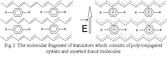
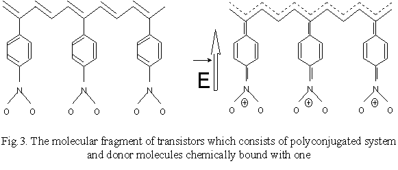
The quantitative characteristics of the initial and final value of transistor conductivity are determined by the number and characteristic of the special molecules and by their susceptibility to external fields or chemical reagents, as well as the character of electron transfer between the one-dimensional conjugate electron system and the electron system of the special molecules.
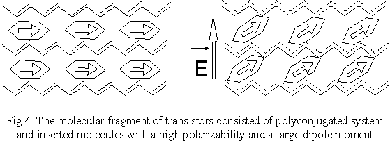
In another approach it is assumed that the device operations based on the interaction between separate one-dimensional molecular systems through the influence of the electrical field on a "guest" special molecule with a high polarizability and a large dipole moment located in the matrix consisting of one-dimensional molecular fragments. Under an internal electrical field (E), on the one hand, the high polarizability molecules affect the one-dimensional electronic system, on the other hand, the equilibrium orientation of the dipole moment of the "guest" molecules is changed. In both cases it is possible to expect the alteration of exchange interactions between neighboring one-dimensional molecular systems, but with different relaxation times. As a result, the electrical conductivity of the compounds on a direction perpendicular to the internal field will be changed. The oversimplified system is illustrated schematically in Fig. 4.
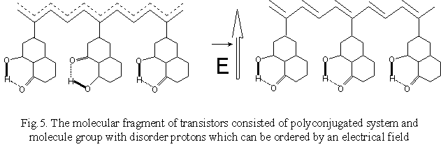
In turn, disorder of the one-dimensional lattice can be obtained by a disorder of the molecular units of which this lattice consists. There can exist both a static and dynamic disorder. Moreover, it can be achieved by a disorder of guest molecules or ions which are located between neighbouring one dimensional systems. A fragment of a molecular structure in which the ordering of protons happens in an operation of an electrical field is presented in Fig. 5.
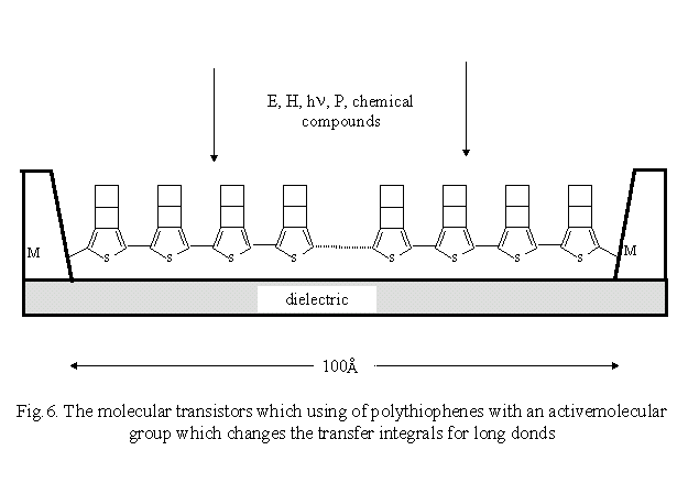
On basis of similar molecular systems simple and effective field transistors can be created. Fig. 6 shows this hypothetical molecular transistor, which using deviations of polythiophenes with an active molecular group which allow us to change the relative transfer integrals for the short and long bonds.
Conclusion
Thus we may conclude the use of the effect instability in one-dimensional electron systems makes it possible to design new devices with high sensitivity to external influence. The phenomenon of electronic instability of one-dimensional molecular systems has a number of properties which make it possible to use this phenomenon as a physical principle for designing molecular electronic devices. Some of them are:
- this phenomena allows the designing of electronic devices with a size of about 50-100 Å;
- the electrical conductivity of such a system can be varied by external fields;
- this allows to control state of one or several identical molecules and conversion their condition in macroscopic conductivity of the one-dimensional systems;
This property will allow us to create molecular electronic devices in the nearest future: molecular transistor; memory cell; chemical sensor; artificial neuron with plastic synapses.
References
- Krieger Ju.H. (1993) Molecular electronics: Current state and future trends. J.Struct. Chemistry, 34, pp. 896-904.
- Krieger Ju.H. (1996) Electronic instability of one-dimensional molecular system as physical principle for design of electronic devices. Extended Abstracts (The Third European Conference on Molecular Electronics, Leuven) pp. 73-76.
*Corresponding Address:
Dr. Juri H. Krieger
Institute of Inorganic Chemistry
Lavrentiev ave. 3, 630090, Novosibirsk, Russia
E-mail: [email protected]
|