Transport Phenomena Investigation
in Nanomaterials
Towards Molecular Devices
Corresponding Address:
Claudio Nicolini, Fondazione EL.B.A.,
Via Medaglie d'Oro 305 - 00136 Rome, Italy
ph: +39 6 35410728, fax: +39 6 35451637,
email: [email protected]
This is a draft paper
for a talk at the
Fifth
Foresight Conference on Molecular Nanotechnology.
The final version has been submitted
for publication in the special Conference issue of Nanotechnology.
This page uses the HTML <sup> and
<sub> conventions for superscripts and subscripts. If
"103" looks the same as "103"
then your browser does not support superscripts. If "xi"
looks the same as "xi" then your browser does not
support subscripts. Failure to support superscripts or
subscripts can lead to confusion in the following text,
particularly in interpreting exponents.
Abstract
A detailed study of several organic-based structures is
reported in this paper. Organic materials with different
electrical properties have been characterized, such as fatty
acids salts used as dielectric materials, charge transfer salts
and conductive polymers used as organic metals. Different
technologies have been utilized in obtaining the samples suitable
for investigations, as Langmuir-Blodgett deposition technique,
electrochemical deposition and layer-by layer adsorption (or
polyelectrolyte self assembling).
Aluminium/ Langmuir-Blodgett film of fatty acids
salts/Aluminium sandwich structures have been constructed; the
sample preparation procedure has been optimized to minimize
problems related to short circuits between upper and lower
electrodes by means of chemical and physical treatments of the
substrate surfaces. The results show that the measured
characteristics are related only to the properties of the films
and wich are in good agreement to the theoretical predictions.
Starting from these results, the behaviour of more attractive
materials have been investigated: conducting polymers (such as
polypyrroles and polyanilines) and metalloproteins (such as redox
enzymes and cytochrome P450) have been studied in order to
highlight their capabilities to develop hybrid structures and
devices. Charge transfer salts and polypyrrole layers deposited
on interdigitate electrodes have been characterized in order to
highlight their electrical properties. The multilayer formation
was controlled by Quartz Crystal Microbalance technique and the
resulting morphology has been investigated by Scanning Tunneling
and Atomic Force Microscopy.
1. Introduction
In the last years, many efforts were performed to investigate
the electronic properties of organic materials and their possible
applications [1, 2]. Bioelectronics and molecular electronics are
two different aspects of this attempt, together with the
technologies suitable to organize the biomaterials, preserving
their activity and functionality [3].
For example, to investigate the electrical properties of
dielectric organic materials, structures composed by a bottom
metal electrode, an intermediate film, and a top metal electrode
are usually created. Often, the organic layer was formed by
Langmuir-Blodgett (LB) technique [4, 5], but a poor deposition of
LB films on metal base electrodes was observed yielding the
authors to propose more complicated structures [6,7]. The use of
aluminium to form both contact elctrodes was proposed by many
authors but recent works demonstrated that, in reality, the
characterizations may be affected by the oxide layers rather than
by the film itself and by short-circuits between the upper and
the lower metal contacts, usually created when the upper metal is
deposited [8].
In this work, we formed Metal/Insulator/Metal (M/I/M) sandwich
structures, transferring monolayers of barium behenate onto the
pre-treated surface of a glass or sapphire substrate, using
evaporated aluminium for both contacts. We believe that the
problem of pinhole influence by the use of a procedure consisting
in a substrate pre-treatment, proposed by ref. 9 for other
purposes have been solved by us. A high dose electron beam
irradation of a first deposited monolayer before the further film
deposition always results in the cross-linking of the molecules;
thus a very strong homogeneous monolayer has been obtained. From
one side, it makes more difficult the penetration of aluminium up
to the bottom electrode under evaporation, from the other side, a
smooth and highly hydrophobic surface is formed. We performed an
AC characterization of the above mentioned structures, optimizing
the junction and contact fabrication. Investigating the DC
conduction properties of the samples, we propose also a transport
mechanism inside the organic dielectric, dependent upon the
magnitude of the applied bias and upon the number of monolayers,
corresponding to the literature data which were obtained with
more complicated solutions.
Among the organic compounds that behaves like organic metals,
we investigated charge-transfer salts and conducting polymers.
Surfactant compounds containing the
bis(ethylene-dithio)tetrathiafulvalene (BEDT-TTF) appear to be
very promising for production of highly conducting LB films
[10,11]. However, the procedures of functional element
preparation are usually complicated and the obtained results, in
our experience, are poorly reproducible. Thus, for a real
application, the technology must be simplified as much as
possible and the reproducibility has to be the first feature. For
this reason, we investigated the realization of layered
nanoarchitectures via directed assembly of anionic and cationic
molecules, as reviewed by ref. 12. In order to highlight the
attractive features of this technique (no dedicated and sensitive
equipment is needed and the adsorption is carried out from
aqueous solutions), we investigated the electrical properties of
polypyrrole deposited on glass slides and interdigitated
electrodes. Polypyrrole is one of the most important electronic
materials among the heterocyclic conducting polymers [13] and one
of the most extensively studied conductive polymers. Polypyrrole
films synthetized in para-toluene sulpnonate (PTS) electrolyte
have been found to have excellent electrical conductivity [14].
When polypyrrole films are in conducting forms, the anions
which are affiliated with the cationically charged polymer
chains, have been found to be 10-35% by weight. The anions such
as p-toluene sulphonate are poorly nucleophylic and permit the
formation of good quality films. The level of oxidation of
pyrrole is 0.25-0.3 per pyrrole unit, corresponding to one anion
for every 3-4 units [15,16]. The recent past has shown the
preparation of in situ-self assembling layer by layer film of
polypyrrole [12]. So, experiments have been carried out with this
polyanion by varying the deposition techniques and the deposition
parameters. Further, the time-dependent electrical properties of
various doped polypyrrole films have been investigated and the
morphology of the samples have been checked with STM and AFM
techniques.
2. Experimental Procedures
2.1 Preparation of dielectric structures
The MIM structures were formed on glass or sapphire slides.
Before metallization, substrates were cleaned and heated at 80
�C with sulphuric acid and then rinsed with deionized water. A
metal pattern consisting of a 1000 �-thick aluminium strips was
then deposited by shadow evaporation under vacuum (10-5
torr), with substrates heated at approximately 200 �C to improve
adhesion. After evaporation, samples were kept at atmospheric
pressure for about 12 hours to obtain a stable aluminium oxide
layer. The barium behenate layers were deposited with a standard
LB system and all deposition parameters are reported in Table 1. At each dipping step a bilayer was
added to the structure, forming samples with different number of
monolayers (from 2 to 40). Transfer ratios were always equal to
1.0 � 0.1. The first monolayer was irradiated by an electron
beam at 1kV, with a dose of about 10-3 Ccm-2,
causing a cross-linking between the molecules, i.e. forming an
uniform, mechanically strong, hydrophobic covering. According to
ref. 14, the thickness of barium behenate monolayer decreases in
a range between 5 � and 10 �.
Table 1. LB
Deposition parameters
| Spreading solvent |
benzene |
| Concentration
of compound |
0.33 mg ml-1
(behenic acid) |
| Surface pressure |
33 mN m-1 |
| Speed of dipping |
5 mm min-1 |
| Rate of compression |
100 mm2
min-1 |
| Subphase |
10-4
(barium acetate in deionized water) |
| Temperature |
20 �C (approximately) |
| pH |
7 |
After the deposition of all the organic layers, a 1000
�-thick top aluminium electrode was then evaporated, with a
careful attention to avoid heating damages of the samples; in
particular, the contact was formed in several steps, evaporating
small quantities of metal at each step. The entire procedure is
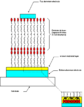
depicted in Figure 1. The final
configuration of the M/I/M structure is shown in Figure
2; the pad surfaces utilized for measurements are of the
order of 0.002 cm2.
[Full size Figure 1: 13K, 684 x 800 pixels]
Figure 1. Schematic representation of the M/I/M
structure described in the text.
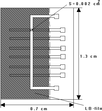
Figure 2. Drawing of a typical sample (not in
scale) incorporating the M/I/M structure of Figure 1. Several
electrodes are first evaporated on a substrate, i.e. glass or
sapphire; the dielectric film is then deposited with the
metodology described in the paper; a single top electrode is
finally evaporated onto the film.
2.2 Preparation of conducting structures
The electrochemical deposition and in situ self-assembling
layer by layer absorption techniques were used for obtaining the
conducting samples. First of all, the substrates were treated
with the following procedure to create charged surfaces. They
were cleaned with a 7:3 concentrated sulfuric acid/hydrogen
peroxide solution and a 1:1:5 ammonium hydroxide /hydrogen
peroxide/ water solution for 1 h; in this way, a hydrophilic
surface was obtained.
The electrochemical deposition of polypyrrole was carried in a
cell consisting of three electrodes, where glass indium-tin-oxide
plate served as working electrode (sheet resistivity 20 Ohmcm),
platinum as counter and AgAgCl as reference electrode. The anodic
deposition of polypyrrole was carried out from 0.1 M pyrrole
monomer in an aqueous solution of 0.1 M sodium salt of
paratoluene sulphonic acid. The polypyrrole films was obtained at
a current density of 0.1 mAcm-2. Various thicknesses
of the polypyrrole films were obtained by varying the time
deposition.
In the layer-by-layer adsorption, to covalently anchor charges
onto the surface, the cleaned slides were immersed for 10 minutes
each into the following solvents: methanol (HPLC grade), 1:1
methanol toluene, and toluene (analytical grade). Then they were
exposed to 5% vol. solution of
(N-2-aminiethyl-3-aminopropyl)trimethoxysilane (TMS) in toluene
for 12 hours. After silanization, the slides were dipped in
boiling toluene for 1 h. The substrates were then dipped for 10
minutes in toluene, 1:1 methanol/toluene and methanol and then
thoroughly washed with deionized water. This procedure produces a
surface with covalently anchored amine group (positively charged
surface).
In addition, the sample was treated with
sulphonated polystyrene (PSS) in order to obtain a negatively
charged surface, suitable for the formation of conducting salts
of polypyrrole (in situ, by simultaneous polymerization of the
monomer and oxidation of the polymer). The supporting solution
was 10-3 M (PSS 90% sodium styrene 4-sulfonate, Mw =
70,000) in deionized water, pH = 1. The active solution of
polypyrrole was made by dissolving an oxidizing agent, ferric
chloride, in deionized water, with pH = 1 by addition of HCl. The
paratoluene sulphonic acid (PTS) was dissolved in the above
solution followed by the addition of pyrrole monomer. The
utilized concentrations for the fabrication of the polypyrrole
films were 0.006 M FeCl3, 0.026 M PTS and 0.02 M
pyrrole. After the addition of pyrrole monomer the solution was
stirred for 15 minutes and filtered. The protonated substrates
were dipped for 10 minutes in PSS solution (to obtain one layer)
and rinsed several times before dipping in the pyrrole solution.
A schematic drawing of the procedure is sketched in Figure 3.
Figure 3. Schematic drawing (not in scale) of a
typical polymer-based conducting structure.
A single layer of polypyrrole, obtained in five minutes,
depends on the surface chemistry of the substrates. The
alternating dipping sequence was repeated to buid alternate
structures. Alternatively, the substrate was also immersed in
polypyrrole dipping solution for several intervals, rinsed and
dried.
2.3 Characterization of conducting structures
The samples were tested with an home-built nanogravimetric
apparatus, in order to check the relationship between deposition
time and an increment of the multilayer thickness. A different
number of layers was transferred onto 10 MHz AT-cut quartz
crystal microbalances with gold electrodes (Nuova Mistral, Italy)
and the decreasing frequency of the polypyrrole multilayers and
of the alternating PSS/polypyrrole structures were analyzed. In Figure 4 a typical result is presented, showing
a linear dependence of the frequency shift versus the deposition
time, as expected. Figure 5 represents the
same result in the case of alternating deposition of
PSS/polypyrrole layers (a deposition step consists of two parts,
the deposition of PSS during 10 min. and the deposition of
polypyrrole during 5 min.). Also in this case, a linear
relationship has been obtained.
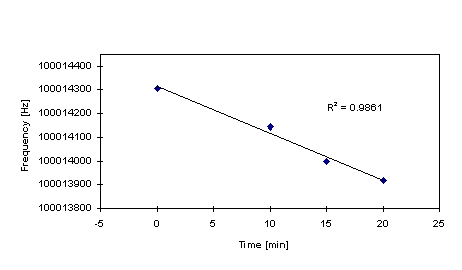
Figure 4. Relationship between frequency variation
and time deposition of polypyrrole samples deposited onto 10
MHz quartzes.
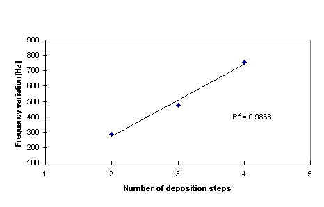
Figure 5. Relationship between frequency variation
and deposition steps of PSS/polypyrrole samples deposited on
10 MHz quartzes.
In addition, the conducting samples surfaces were
investigated by a home-built Atomic Force Microscope working in
air and by a Scanning Tunneling Microscope (AsseZ-MDT, Italy). Figure 6 shows examples of this type of
investigation: the left images refer to STM analysis while the
right ones refer to AFM characterization. In part (a) the
morphology of a typical sample obtained by layer-by-layer
technique has been reported: the surface is organized in
spherical objects (grains) of about 300 � in diameter. The image
sizes are 0.5 x 0.5 �m.
In part (b) the organization of a sample obtained
by electrochemical deposition has been shown: in this case the
surface presents a cluster morphology. The aggregates present fine
structures inside, like to those obtained in the above pictures.
The STM image has a size of 0.5 x 0.5 �m, while the AFM image
has a size of 2.2 x 2.2 �m.
Figure 6. Morphological investigation by Scanning
Probe Microscopes to characterize the surfacial morphology
obtained by layer by layer and electrochemical techniques.
The left images refer to STM analysis while the right ones
refer to AFM characterization.
In part (a) the morphology of a typical sample obtained by
layer-by-layer technique has been reported: the surface is
organized in spherical objects (grains) of about 300 � in
diameter. The image sizes are 0.5 x 0.5 �m.
In part (b) the organization of a sample obtained by
electrochemical deposition has been shown: in this case the
surface presents a cluster morphology. The aggregates present
fine structures inside, like to those obtained in the
above pictures. The STM image has a size of 0.5 x 0.5 �m,
while the AFM image has a size of 2.2 x 2.2 �m.
2.4 Electrical measurements
For the electrical characterization, glass substrates and
substrates with 50 pairs of chromium interdigitates electrodes
have been used (each pair is spaced to 50 �m and each track is
50 �m in width, 5 mm in length and 40 nm in height).
The electrodes were contacted by tungsten tip probes connected
to a micromanipulator control (PH 100, Karl Suss, Germany). The
probes were connected to the measuring instrumentation by short
shielded cables.
For the M/I/M structure, AC measurements were performed with a
precision LCR meter (HP 4284A, Hewlett Packard, USA). The study
was directed to understand the behaviour of these structures
varying the number of bilayers, the applied bias potential and
the frequency of the applied AC signal (the amplitude of the AC
signal applied across the structures was usually equal to 150
mV).
The DC experiments were performed using a Keithley
electrometer (model 6517). Normally, fatty acids salts behave
like good insulators, with dielectric strenghts greater than 106
V cm-1. However, like in real dielectric materials,
according to the temperature and bias potential, a transport
phenomenon can be obtained.
Both the instruments were driven by a PC through a GPIB
interface, with a home-made software (this solution allowed a
fast data acquisition and an easy programming of the
instruments).
For the conducting structures, the current/voltage
characteristics were obtained by biasing the structure with a
16-bit resolution I/O board (National Instruments, mod. PCI MIO
16XE10) and measured by the Keithley electrometer.
3. Results and discussion
3.1 Electrical behaviour of M/I/M structures
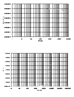
According to our AC measurements, between 20 Hz and 10 KHz,
the capacitance of the Al/LB fatty acid salts/Al is almost
independent on frequency, while for higher values it decreases,
according to the following expression:

Data from literature confirm this dependence on frequency,
which could depend either on permanent or induced dipoles or on
hopping electrons in the dielectric material.
Conductance measurements can be modeled by the following
expression:

In Figure 7 this type of behaviour is
shown. We obtained also a linear dependence of 1/C versus the
number of layers demostrating the reproducibility of a monolayer
capacitance and hence for one monolayer to the next. For the
interfacial layer a capacitance of the order of 800 pF was
obtained; if we assume that this layer has an average dielectric
constant = 4.5 (native oxide), its thickness is of the order of
few nanometers (as reported in refs. 6).
[Full size Figure 7: 19K, 664 x 752 pixels]
Figure 7. AC behaviour of the realized M/I/M
structures. A detailed comparison of this dielectric
phenomena characterization with similar ones published by
other groups shows a good agreement; differences within the
data are of the order of 5% (that is, of the same order as
the accuracy in producing the electrodes and measuring their
areas).
In addition, to identify the conduction processes through the
LB layers, the shape of their I/V characteristics was compared
with that expected from theoretical considerations of the
conduction processes through inorganic insulating films [17].
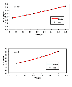
It was found that the I/V characteristics obey
the I exp (Vn) relationship, with
n depending on the insulating layer thickness (N): in Figure 8, plots of ln (I) versus Vn
are shown. Figure 8(a) refers to a bilayer (n 0.5) while Figure 8
(b) refers to 8 monolayers of barium behenate (high applied
field, n 1). Two transport phenomena can explain our experimental
observations: if n 0.5, the conduction process arises mainly from
the injection of carriers from the electrodes over the potential
barrier formed at the metal-insulator interface (Schottky
mechanism); if the film thickness increases, the conduction due
to the Schottky mechanism can be negligible and charges are
excited out of traps in the insulating film. The DC conduction in
thicker multilayers structures is essentially determined by
defects in the LB layers and obey to the Poole's law, based on
the classical calculation of ionic conductivity [18]
[Full size Figure 8: 6K, 664 x 676 pixels]
Figure 8. Dependence of ln (I) versus Vn
of samples consisting of 2 (part A) and 8 (part B) monolayers
of barium behenate. Different transport mechanisms for the
two samples and in general for samples of different thickness
drive the carriers in the insulating layers, as proved in the
text.
3.2 Electrical conductivity on polypyrrole samples
We performed first the electrical measurements of doped
polypyrrole films on glass substrates, simply by contacting two
different points of the sample. Then, in order to not introduce
some problems related to the contacts, we deposited the same
samples on interdigited electrodes with the perspective that the
interdigited chromium electrode metals do not diffuse in
polypyrrole films and the interdigited electrodes have fixed size
and equal separation from one strip to another. We carried out
the electrical measurements on such type of interdigited
electrodes depositing, with different procedures, various numbers
of layers. First of all, we checked the behavior of the current
versus voltage (I/V) curve. Figure 9 (part
A) shows the I/V curve of a polypyrrole sample obtained via
electrochemical deposition: the I/V curves do not show an ohmic
behavior and the conductivity varies with time. Part B shows the
same characterization performed on a sample deposited with
layer-by-layer absorption: the ohmic behavior and the
conductivity values are retained for 30 days time period. The
conductivity of the samples ranges between 10-1-10-2
S/cm according to their thickness. The thickness values have been
estimated via AFM by imaging samples with ad-hoc deposited steps
of organic material.
Figure 9. Part (A) shows the dependence of I
versus V for a polypyrrole sample deposited via
electrochemical technique. The sample shows a non-ohmic
behavior and unstability in time. Part (B) shows the
dependence of I versus V of a polypyrrole
sample deposited via layer by layer technique. The ohmic
behavior and the stability are mantained during a month of
testing.
The I/V characteristics versus number of layers and the effect
of dopants on the electrical conductivity on these films are
actually under study; preliminary results show a gradual
increment in the current magnitude according to the increment in
the number of layers, probably linked to an increase in the
charge defects in the conducting films. In addition, the doping
procedure can introduce some unstability in I/V characteristic,
and the magnitude of the current seems to reach a saturation
level.
4. Conclusions
The paper deals with the investigation of the properties of
organic compounds in order to highlight the possibility of their
use in the development of real organic devices. The stability in
time, the reproducibility of the procedure for deposition and the
simple deposition technique are, in our opinion, the key points
to focus for testing any practical application of these
materials. So our approach was focused to investigate well known
materials and technologies keeping in mind the final goal to
realize a real device.
A new series of experiments are currently being performed to
incorporate monolayers of biological molecules such as redox
enzymes in order to investigate the electrical properties of
hybrid structures and devices.
Acknowledgments
The authors would like to thank Dr. M. Sartore for his
important help in providing the software programs interconnecting
the PC and all the measuring instruments, Dr. M. Salerno for AFM
characterizations and Mr. R. Galletti for software support.
References
[1] Peterson I R 1992 Nanostructures based on molecular
materials (Weinheim: VCH) p 195
[2] Stoldt M, B”uerle P, Schweizer H and Umbach E 1992 Nanostructures
based on molecular materials (Weinheim: VCH) p 295
[3] Nicolini C 1996 Molecular Bioelectronics (Singapore
and New York: World Publishing C.)
[4] Tieke B 1990 Adv. Mater. 2 (5) 222
[5] Petty M C 1991 J. Biomed. Eng. 13 209
[6] Geddes N J, Sambles J R, Parker W G, Couch N R and Jarvis
D J 1990 J. Phys. D: Appl. Phys. 23 95
[7] Roberts G G, Vincett P S and Barlow W A 1978 J. Phys.
C: Solid State Phys. 11 2077
[8] Procarione W L and Kauffman J W 1974 Chem. Phys. Lipids
12 251
[9] Feigin L A, Lvov Yu M and Troitsky V I 1989 Sov. Sci.
Rev. A Phys. 11 285
[10] Berzina T S, Troitsky V I, Stussi E, Mul� M and De Rossi
D 1993 Synt. Metals 60 111
[11] Troitsky V I, Berzina T S, Katsen Ya Ya, Neilands O Ya
and Nicolini C 1995 Synt. Metals 99
[12] Decher G 1996 Comprehensive Supramoleculars Chemistry
Vol. 9 "Templating, Self-Assembly and
Self-Organisation" (Oxford: Pergamon Press) p 507
[13] Fukuyama M, Kudoh Y and Yoshimura S 1993 Mol. Cryst.
Liq.Cryst. 224 61
[14] Batz P, Schmei�er D and Gopel W 1990 Solid State
Commun. 74 461
[15] Salmon M, Diaz A F, Logan A J, Krounbi M and Bargon J
1983 Mol. Cryst. Liq.Cryst. 83 203
[16] Imanishi K, Satoh M, Yasuda Y, Tsushima R and Aoki S 1988
J. Electroanal. Chem. 242 203
[17] Sze S M 1981 Physics of Semiconductor Devices (New
York: John Wiley & Sons)
[18] Bockris J O'M and Reddy A K 1973 Modern
Electrochemistry (New York: plenum Rosetta Edition) 387
|