Nanofabrication of Unijunction Transistors
based on Metallophthalocyanines
by
Gordon A. Parker, K.O. Park
Corresponding Address:
For comments please contact [email protected]
This is a draft paper
for a talk at the
Fifth
Foresight Conference on Molecular Nanotechnology.
The final version has been submitted
for publication in the special Conference issue of Nanotechnology.
This page uses the HTML <sup> and
<sub> conventions for superscripts and subscripts. If
"103" looks the same as "103"
then your browser does not support superscripts. If "xi"
looks the same as "xi" then your browser does not
support subscripts. Failure to support superscripts or
subscripts can lead to confusion in the following text,
particularly in interpreting exponents.
Abstract
In this thought experiment, the electrical conductivity modulation of unijunction transistors (UJT's) based on metallophthalocyanines, such as CuPc, PbPc, and Cu(PcF8)/NiPc, which are deposited onto P+ region of a n-type substrate is described. The three different kinds of unijunction transistor could be fabricated using a imprint nanolithography and a sublimed method along with a conventional microelectronic fabrication technique. They are called MPc unijunction transistors, denoted by MPcUJT(M=Pb, Cu) and by Cu(PcF8)/NiPcUJT, where Cu(PcF8)/NiPc is a bilayer to be deposited onto P+ region of a n-type substrate. A switching voltage of Cu(PcF8)/NiPc unijunction transistor (UJT) to be fabricated from this experiment could be larger than that of a conventional unijunction transistor due to large forward diode drop from a bilayer of Cu(PcF8)/NiPc of the P+ region in Cu(PcF8)/NiPcUJT.
It is also expected that the switching voltages of CuPcUJT and PbPcUJT to be fabricated by doping with NO2 would be smaller than those of CuPcUJT and PbPcUJT to be fabricated by doping with O2. The switching time of the fabricatedUJT from this work would be smaller than that of a conventional UJT adjusting the length from the P+ region to the source.
A unijunction transistor with a property of an S-shaped curve (Input vs. Output), which would be useful for neural network, could also be fabricated from this experiment.
I. Introduction
Phthalocyanine (Pc) and other metallo macrocycle molecules have been extensively studied and applied to interdigital electrodes, Langmuir Blodgett films, surface acoustic wave devices, and insulated gate field effect transistors. Metallophthalocyanines (MPc's) are a class of coordination compounds which are currently receiving a great deal of attention due to their interesting  electronic characteristics (15). The physical and chemical properties of MPc's have been studied with a large literature (16-18) of more than several thousand publications. electronic characteristics (15). The physical and chemical properties of MPc's have been studied with a large literature (16-18) of more than several thousand publications.
Molecular electronic devices using phthalocyanine molecules were first discussed at the workshop held in Washington D.C., in 1981, organized by the late Forest Carter (14).
Phthalocyanines can also be considered as a model system for the important biological molecules, such as hemoglobin and chlorophyll. Phthalocyanine molecules are P type semiconductors with a typical energy gap of about 1.8 ev. (14). Their semiconducting and structural properties resemble those of doped polyacetylenes, and the characteristic forms of phthalocyanine molecules are monomer or aggregated units, ring stacked or polymeric sheet type (14).
The electrical and optical properties of phthalocyanine molecules depend strongly on structural configuration (14).
The concept of electrical conductivity modulation (current (I) vs voltage (V)) has been suggested with the use of a N channel depletion type MOSFET's (metal oxide semiconductor field effect transistor) with metal containing phthalocyanine Langmuir-Blodgett films (1,2).
Metallophthalocyanines (MPc's) have been of great interest due to their -electron interactions. Many MPc's are known to show p-type semiconducting electronic properties when exposed to an oxygen-containing atmosphere (4).
The role of oxygen is shown to partially dope the material, which creates delocalized holes as the charge carriers (3). Most MPc's are water and air stable, thermally stable, and nontoxic. They can be sublimed or sputtered with highly uniform, thin films on a variety of substrates (3). Their synthetic literature is vast, and they are also relatively inexpensive and easy to prepare (3). The general properties of phthalocyanine molecules have been discussed in other reports. However, some basic and relevant properties are presented again here.
The basic 18 electrons in metal free and other MPc molecules have rich molecular orbitals and available energy levels due to the free-electron gas model.
The energy difference between the highest occupied and the lowest empty state is given by solving schrödinger equation (19).
The size of the microcrystals (or nanocrystals), the temperature, the humidity, the state of material purity, all influence the rate of migration of 02 in the MPc thin films (4).
Mixed MPc thin films have also been obtained by co-sublimation of two MPc's under high vacuum, and VOPc acts as a dopant towards CuPc in the mixed polycrystalline thin films VOPc-CuPc (4). When PbPc is doped with O2, the photocurrent is multiplied by a factor of more than 100 with similar results found in single crystal or thin films of CuPc (4).
Id-Vg (drain current vs. gate voltage)characteristics of undoped trans-(CH)x MESFET (metal semiconductor field effect transistor) at Vds=-10V (for planar type)shows the inversion of an S-shaped curve (5). This unique property would be investigated in more details for the next subject.
A polymeric phthalocyanine, such as pCuPc, plays a role in improving the electrical conductivity of the polyimide, on the heat treatment, which is known to have excellent mechanical and thermal properties (6).
The central metal atoms of MPc's form a one dimensional molecular metal, a potentially important class of conductors (7).
The inversion of the rectifying property of the Al/PbPc/Au structure in air and vacuum, by the conventional vacuum evaporation, was observed (8). The Al/CuPc/Au structure showed the rectifying property in air, but no remarkable change of the rectifying property in vacuum (8).
PbPc could be expected to have unique properties due to the one-dimensional structure. However, the fundamental properties of the PbPc films have not been reported in detail (8).
The electrical characteristics of an insulated gate field effect transistor (FET) based on an intrinsic molecular semiconductor, Pc2Lu were described with threshold voltage, transconductance, and amplification factor (9).
To deposit single molecules of CuPc on a GaAs surface, R. Möller et. al. have used the tunneling tip (10). The scanning tunneling microscope (STM) could be used to deposit single molecules of MPc's on a semiconductor surface and to measure current-voltage characteristics on an atomic scale (11).
The attachment of CuPc molecules to graphite changes the electrical characteristics of the STM from relatively symmetric to highly asymmetric or rectifying due to the asymmetry arising from the electronic energy levels of the CuPc (12). Bulk electrical properties do not follow directly from the molecular domain (13). For example, macroscopic conductivity measurements of doped polyacetylene don't probe single molecules properties because its bulk conductivity is limited not by carrier mobility in a molecule but by interchain hopping (13).
The definition of electrical conductivity of a single molecule is not obvious. Nevertheless, under particular circumstances molecules could behave in a manner analogous to that of familiar macroscopic devices and materials (13). For this purpose, there could be a number of important switching applications which require that a device (probably, a nanoscale device) remain in the off state under forward bias until switched to the on (conducting) state by an external voltage. A bulk (or nanoscale) device is typified by a high impedance (off condition) under forward bias until a switching signal is applied. The device could exhibit low impedance (on condition) after switching.
A switching device (bulk or nanoscale device) which operates by electrical conductivity modulation should be presented.
A model device which we describe is a unijunction transistor (UJT) switching from a off state to a on (conducting) state when the applied voltage reaches a critical value.
The equivalent circuit representation
(23,25) of a unijunction
transistor is shown in Fig.
1.
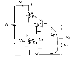
[Figure 1] Equivalent circuit of a unijunction
transistor.
This model device could be useful in various switching applications, including timing circuits, and in triggering other devices.
The S-shaped curve of the current vs. voltage, which is useful for neural net, could be studied and discussed from the future experiment.
A nanofabrication method of the UJT's could also be discussed and presented in the next section.
II. Nanofabrication Method of Unijunction Transistors
It can be suggested that there are two phthalocyanine film deposition techniques commonly used (18). Vacuum sublimation is used for most unsubstituted phthalocyanine compounds. The Langmuir-Blodgett (L-B) film transfer technique may be used for phthalocyanine compounds which are usually substituted at the axial or peripheral positions.
The L-B film transfer technique based on metal oxide semiconductor field effect transistors (MOSFET's) had been discussed in the previous publication (2). In this experiment, phthalocyanine vacuum sublimations are to be conducted by heating a small quantity of purified material at variable temperature ranges at reduced pressure in an inert atmosphere or under vacuum.
It is well known that the morphology of the phthalocyanine films is variable and strongly depends on the sublimation conditions.
Although oxygen has a demonstrated effect on the electrical conductivity of phthalocyanine crystals and films, it is quite small. MPc's can be prepared as a uniform thin film via solution-grown method (20) or evaporation, but evaporation or powdered MPc (21) is inferior to single crystal MPc in the electrical conductivity by a factor of several orders of magnitude.
Nitrogen dioxides, such as monomeric NO2, and dimeric N204 are somewhat complicated gas which exists in a strongly temperature-dependent equilibrium.
In our experiment, PbPc, and CuPc films are to be prepared on a n-type substrate by the usual sublimation technique using PbPc, and CuPc powders.
The I-V characteristics of aUJT would be affected by doping with O2 and NO2.
To nanofabricate a typical UJT, we use imprint lithography with 25-nanometer (25) resolution which is based on compression molding and a pattern transfer process. The mold can be made of metals, semiconductors, or dielectrics, and reactive ion etching (RIE) can be used to transfer the thickness contrast pattern created by imprinting through the entire resist thickness (22). Our experiments could use silicon dioxide or metal molds on a n-type substrate. The mold can be patterned with lines or dots with a minimum lateral feature size of 25nm by means of electron beam lithography (22). In imprint lithography technique, a mold with nanometer-scale or micrometer-scale features is first pressed into a thin resist cast on a n-type substrate.
A proposed imprint lithography could have many advantages (22) over conventional lithographies.
The use of an energetic beam of electrons, photons, or ions, which creates a chemical structure contrast in a resist, can be abandoned (22). It also eliminates many factors that limit the resolution of conventional lithographies, such as wave diffraction, scattering in the resist, backscattering from the substrate, and chemistry of resists and develops (22).
In this work, the three different kinds of UJT could be fabricated using an imprint lithography and a sublimed method along with a conventional microelectronic fabrication technique. They are called MPc unijunction transistors, denoted by MPcUJT (M=Pb, Cu) and by Cu (PcF8)/NiPc UJT, where Cu(PcF8)/NiPc is a bilayer to be deposited onto P+ region of a n-type substrate. If we assume that P+ region of a UJT to be fabricated in our experiment is composed of MPc(M=Pb, Cu, Ni, etc.) and the n-type base region composed of Si, the switching potential VB of the UJT could have a greater value compared with that of a conventional UJT commercially available, due to a unusually large diode drop, which is the switching on potential in the forward bias region.
Results and Discussion
A bilayer of Cu(PcF8)/NiPc (3) shows an unusually large diode drop, which is the switching on potential in the forward bias region. Therefore, its I-V characteristics of Cu(PcF8)/NiPcUJT with B (iB=0) open and with iB present is shifted toward VB, a switching voltage of Cu(PcF8)/NiPcUJT as shown in Figure II. A switching voltage (Vs) of Cu(PcF8)NiPc UJT to be fabricated from our work could be larger than that of a conventional UJT (VB) due to large forward diode drop from a bilayer of Cu(PcF8)/NiPc of the P+ region in Cu(PcF8)/NiPc UJT, as shown in Figure II.
It is also expected that the switching voltages of CuPcUJT and PbPcUJT to be fabricated by doping with NO2 would be smaller than those of CuPc UJT and PbPcUJT fabricated by doping with O2, as shown in Figure III. The numerical values of the switching voltages, such as Vs, VB, Vc, NO2, and Vc, O2, could be determined experimentally. For iB=0, a UJT functions as a simple PN diode showing a conventional I-V property of a PN diode as shown in Figure II (a). In this case (iB=0), it could be possible that we would fabricate a UJT with a property of an S-shaped curve (1-2) (input vs. ouput) as shown in Figure IV (a). A more detailed design procedure and a nanofabrication method for this device would be a next subject in the near future work. A saturated I-V characteristics (S-shaped curve) of CuPcUJT (or PbPc UJT) could also be obtained from this experiment, as shown in Figure IV.
In mesoscopic physics, the electronic properties of nanometer to micrometer-scale devices have been interesting research area during the last decade. This field has not only studied quantum mechanical properties but also has developed fabrication techniques for attaching wires to small pieces of material (24).
If the deposition of several monomolecular MPc layers onto P+ region of a n-type substrate could improve the efficiency of the minority carrier injection, we would expect that the switching time of a UJT fabricated from this work could be smaller than that of a conventional UJT adjusting the length from the P+ region to the source.
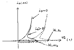
[Figure II] I-V
characteristics with B open and with iB present
(iB>0).
(a), (b); I-V characteristics of a conventional UJT.
(S),(B); I-V characteristics of Cu(PcF8)/NiPcUJT under an atmosphere of
dry, deoxygenated argon.
Vs: a switching voltage of a conventional UJT VB; a switching voltage of
Cu(PcF8)/NiPcUJT. Horizontal arrows mean the curves of (a) and (b) are
shifted towards the ones of (S) and (B).
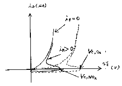
[Figure III].
I-V characteristics of PbPcUJT (or CuPcUJT)fabricated by
doping with NO2 and O2.
Vc, NO2; a
switching voltage of PbPc UJT (or CuPcUJT) fabricated by
doping with NO2.
Vc, O2; a
switching voltage of PbPcUJT (or CuPcUJT) fabricated by doping
with O2.
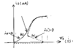
[Figure IV](a) An S-shaped I-V characteristics with B open
(iB=0); (b) A saturated I-V characteristics with
iB present
(iB>0).
References
1. K.O. Park, International Symposium on nonlinear optical
materials, University of
Texas, El Paso, Texas, October 1990.
2. K.O. Park, Nonlinear Optical Materials, eds by H. Kuhn and J.
Robillard, CRC, 75,
1992.
3. T.L. Anderson, G.C. Komplin, and W.J. Pietro, J. Phys. Chem.,
97, 6577-6578, 1993.
4. J. Simon, J. J. Andre, Molecular semiconductors; J.M. Lehn;
C.W. Rees, eds.;
Springer-Verlag, Berlin, 1985.
5. Y.C. Chen, C-C Cheng, M-H, Chen, and K-C Huang; Japanes
Journal of Applied
Physics, Vol. 30, No. 9A, 2101-2106, Sept., 1991.
6. S. Venkatachalam, T.M. Vijayan, S. Packirisamy; Makromol.
Chem., Rapid Commun.
14, 703-706, 1993.
7. M.L.M. Rocco, K.H. Frank, P. Yannoulis; and E.E. Koch, J.
Chem. Phys. 93 (9), 1 Nov.,
1990.
8. K. Kumazawa and M. Yamanaka, Japanese Journal of Applied
Physics, Vol. 30, No.3,
530-531, March, 1991.
9. R. Madru, G. Guillaud, M. Alsadoun, M. Maitrot, J.J. Andre,
J. Simon and R. Even,
Chemical Physics. lett., 145, 343-346. 1988.
10. R. Möller, R. Coenen, A. Esslinger, and B. Koslowski,
J. Vac. Sci. Technol, A8(1),
Jan/Feb., 1990.
11. K.O. Park, Nanofabrication of MOSFET's with metal containing
Pc's, proposal for
Advanced Technology Program, National Institute of Standards and
Technology, June,
1994.
12. M. Pomerantz, A. Aviram, R.A. McCorkle, L. Li, A.G. Schrott,
Science, Vol. 255,
reports 1115-1118, 28 February, 1992.
13. D.H. Waldeck, and D.N. Beratan, Science, Vol. 261, 576, 30
July, 1993.
14. B. Simic-Glavaski, Molecular Electronics I, II, phthalocyanine based Molecular
Electronic Devices, 123-162, North Holand, 1993.
15. K.O. Park, Current Research Areas in the future development,
International
Molecular Electronics, Inc. 1995.
16. Boucher, L.J., Coordination Chemistry of Macrocyclic
Compounds, Plenum, New
York, 1979.
17. Berezin, B.D., Coordination Compounds of porphyrins and
phthalocyanines; J. Wiley
and Sons, New York, 1981.
18. C.C. Leznoff and A.B.P. Lever, Phthalocyanines properties
and Applications, VCH,
UK, 1989.
19. H. Kuhn, Helv. Chim. Acta, 31, 1441, 1948.
20. S. Nakamura, T. Ozaki, et. al., Japanese Journal of Applied
Physics, 28, 991-995,
1989.
21. S. Nakamura, H. Amatatsu, T. Ozaki, S. Yamaguchi, and G.
Sawa, Japanese Journal
of Applied Physics., 830-833, 1988.
22. S.Y. Chou, P.R. Krauss, P.J. Renstrom, Science, 272, April
5, 1996.
23. Ben G. Streetman, Solid State Electronic Devices, 2nd ed.
Prentice-Hall, Inc., N.J.,
1980.
24. L. Kouwenhoven, Science, 275, 1896, 1997.
25. Jacob Millman, Christos C. Halkias, Electronic Devices and
Circuits, McGraw-Hill
Kogakusha, LTD, 1967.
|