Silicon-Based Molecular Nanotechnology
by
Mark C. Hersam*, Nathan P. Guisinger, and Joseph W. Lyding
Department of Electrical and Computer Engineering and Beckman Institute
for Advanced Science and Technology
University of Illinois at Urbana-Champaign, Urbana, Illinois 61801 USA
*[email protected]
http://tm.uiuc.edu/~mark/
This is a draft paper for the
Seventh
Foresight Conference on Molecular Nanotechnology.
The final version has been submitted
for publication in the special Conference issue of Nanotechnology.
Abstract
One potential application of molecular nanotechnology is the integration of molecular electronic function with advanced silicon technology. One step in this process is the tethering of individual molecules at specific locations on silicon surfaces. This paper reports the fabrication of arrays of individual organic molecules on H-passivated Si(100) surfaces patterned with an ultra-high vacuum scanning tunneling microscope (UHV STM). Feedback controlled lithography (FCL) is used to create templates of individual silicon dangling bonds. Molecules introduced in the gas phase then spontaneously assemble onto these atomic templates. Norbornadiene (NBE), copper phthalocyanine (CuPc), and C60 molecular arrays have been made by this technique and studied by STM imaging and spectroscopy. Both NBE and CuPc molecules appear as depressions in empty states images, whereas in filled states images they are nearly indistinguishable from Si dangling bonds. Furthermore, the four-fold symmetry and central copper atom of CuPc are clearly observed at positive sample bias. Spatial tunneling conductance maps of CuPc illustrate charge transfer from the surrounding substrate when the molecule is bound to the surface via its central copper atom. On the other hand, when the CuPc molecule interacts with the substrate via an outer benzene ring, molecular rotation is observed. C60 molecules display intramolecular structure in topographic images and spectroscopic data. The local density of states (LDOS) of C60 clearly shows the location of the lowest unoccupied molecular orbital (LUMO), which suggests that the highest occupied molecular orbital (HOMO) is located within ~0.3 eV of the fermi level.
1. Introduction
Molecular electronics is currently one area being studied as a potential successor to conventional silicon-based electronics technology [1]. One aspect of molecular electronics is the fabrication of devices whose function is governed by single molecules. Though quite promising, single molecule devices present fundamental new challenges, thereby placing estimates of their mainstream applications around the middle of the 21st century (see Figure 1). Nevertheless, tools such as the ultra-high vacuum scanning tunneling microscope (UHV STM) are available to begin exploring this fascinating field. This paper describes a new approach for creating arrays of individual molecules with atomic precision on the technologically important Si(100) surface. The merger of molecular electronics with silicon-based technology represents a hybrid approach with potential near-term applications. The approach described in this paper is that of utilizing the chemical contrast between clean and hydrogen passivated Si(100) to create templates for molecular adsorption. For this purpose a variant of the hydrogen resist STM nanolithography technique [3], termed feedback controlled lithography (FCL) is used to generate arbitrary arrays of individual dangling bonds on the Si(100)-2X1:H surface. The surface is then dosed with appropriately chosen organic molecules that will bind only at the pre-patterned dangling bond sites [4]. Previous STM studies of norbornadiene (NBE) [5], copper phthalocyanine (CuPc) [6,7], and C60 [8-13] suggest the compatibility of these molecules with the experiments of this paper.
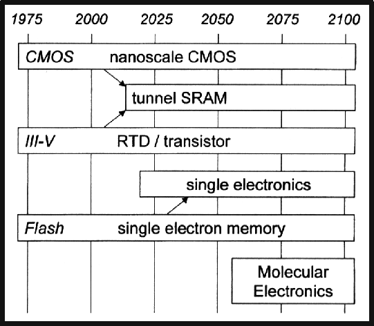 |
| Figure 1. Timeline of anticipated eras for future electronic technologies. This figure is reproduced from the Proceedings of the IEEE [2]. |
Many single molecule analysis techniques have been developed that make use of the STM [14]. By measuring the tunneling conductance [15] and the second derivative of the tunneling current [16], information about the electronic local density of states (LDOS) and vibrational spectra respectively can be obtained with nanometer precision. In this work, constant current topographic images and tunneling conductance imaging are employed to study single molecule rotation [17] and electronic structure. In particular, bias-dependent imaging is performed on NBE arrays, molecular rotation is observed for CuPc, and intramolecular electronic structure is detected for C60. By combining FCL with STM analysis, molecules can be empirically screened for their potential utility in molecular electronic device applications.
2. Feedback controlled lithography (FCL)
The UHV STM hydrogen resist nanolithography technique was originally developed as a method of creating atomic scale lines of clean silicon by desorbing hydrogen from a Si(100)-2X1:H surface [3]. By operating the STM under feedback control, a controlled dose of electrons can be written along a line or over an area to locally depassivate the surface. Although high resolution is achieved, the writing conditions and precise geometry of patterned nanostructures vary with changes of tip structure. This presents a problem for single molecule studies where it is desirable to create precise templates of individual dangling bonds as molecular adsorption sites. Feedback controlled lithography (FCL) was developed as a method to routinely create arrays of single dangling bonds. FCL works by actively monitoring the STM feedback signal (i.e., the tip position) and the tunneling current during patterning, and immediately terminating the patterning conditions when a desorption event occurs. This is illustrated in Figure 2(a) for a desorption event that is triggered by writing conditions of 2 nA and a sample bias of 3 V. Upon desorption, the tip retracts approximately 1.5 Å due to the enhanced local density of states of the depassivated dangling bond, and the tunneling current also momentarily increases until the feedback stabilizes it back to the setpoint value. This distinctive behavior, indicative of an individual desorption event, is easily detected, and thus enables the fabrication of well controlled arrays of isolated dangling bonds as shown in Figure 2(b).
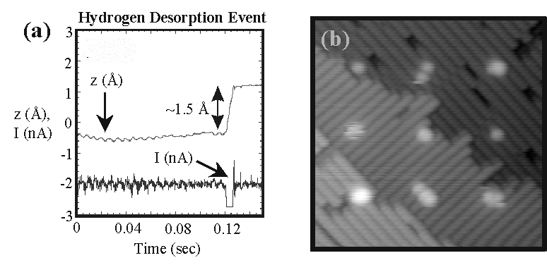 |
| Figure 2. (a) The feedback (z) and tunneling current (I) signals are monitored as a function of time while patterning at 3V, 2 nA. Desorption is clearly observed as a ~1.5 Å step in z. (b) Example of a 3X3 array of depassivated sites created with the FCL technique. The STM image is 170 Å X 170 Å and was measured at -2 V, 0.1 nA. |
3. Molecular arrays
The strong chemical contrast between clean and H-passivated Si(100) allows for selective binding of organic molecules to the STM-patterned clean areas [4]. With FCL this methodology is given an atomic precision handle. In this paper, three organic molecules, norbornadiene (NBE), copper phthalocyanine (CuPc), and C60 have been chosen because of their excellent chemical stability and ease of handling. NBE has a high vapor pressure and is therefore introduced to the UHV environment via a leak valve, whereas CuPc and C60 are low vapor pressure solids that can be sublimated in situ at a temperature of ~300°C [7, 9]. NBE was selected because its two carbon-carbon double bonds (see Figure 3(a)) are expected to react with adjacent depassivated Si(100) dimers by means of a cycloaddition reaction [4]. The distinctive four-fold symmetry of CuPc (see Figure 3(b)), with its peripheral benzene rings surrounding the central Cu, makes it well suited for identification in STM experiments. Finally, the unique truncated icosahedron structure of C60 (see Figure 3(c)) makes its identification by STM straightforward.
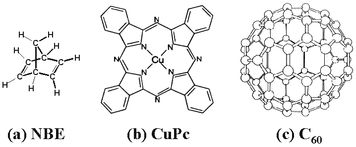 |
| Figure 3. Schematics of the organic molecules studied in this paper: (a) norbornadiene (NBE), (b) copper phthalocyanine (CuPc), and (c) C60. |
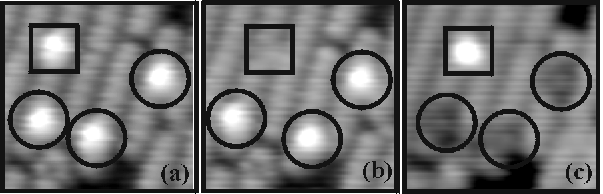
Figure 4 shows the results of isolation of individual NBE molecules. After creating four depassivated sites by FCL (Figure 4(a)), the sample was exposed to a 0.01 L dose of NBE in situ. Figure 4(b) shows the same area after the dose in which one of the sites appears as a slight depression (see box) and the other three (circled) appear as protrusions. In an empty states image, Figure 4(c), this behavior reverses with the boxed site appearing bright and the circled sites appearing as depressions. Since dangling bonds appear bright in both filled and empty states, these images show that a reaction has occurred at each site. The behavior exhibited by the boxed site is consistent with an isolated water molecule on Si(100) [18]. Trace water is a common background constituent in UHV systems. The three boxed sites, on the other hand, represent individual NBE molecules. The ability to distinguish between different surface species is an important strength of combined STM topographic and spectroscopic imaging.
larger image |
| Figure 4. A series of 45 Å X 45 Å constant current (0.1 nA) STM images. (a) Four depassivated sites created via FCL. (b) Filled states and (c) empty states images of the same area after exposure to ~0.01 L of NBE. Note that the boxed site is a depression in filled states and a protrusion in empty states, whereas the circled sites display the opposite behavior. |
4. Copper phthalocyanine results
4.1. Conformation and rotation of CuPc
Figure 5(a) shows an STM image (sample bias = 2 V) after individual depassivated sites created with FCL were exposed to a sublimed flux of CuPc. The molecule on the left side of the image (#1) clearly shows four-fold symmetry, and the central Cu atom appears bright. It should be noted that the appearance of CuPc as a depression in empty states images has been previously observed and explained [7]. The silicon surface immediately surrounding molecule #1 appears slightly brighter than the background, which suggests that the presence of CuPc disrupts the electronic structure of the silicon surface. When the sample bias is reduced to 1.5 V (Figure 5(b)), molecule #1 retains its general structure but decreases in apparent size to the expected 16 Å molecular diameter of CuPc. Overall, the four-fold symmetry and measured diameter are in accord with the molecular dimensions of CuPc suggesting that molecule #1 is being rigidly bound to the surface by its central Cu atom.
Molecule #2 in Figure 5(a) displays radial, rather than four-fold, symmetry. Furthermore, the silicon surface surrounding molecule #2 appears less perturbed (i.e., not as bright) as was seen with molecule #1. In Figure 5(b), molecule #2 retains its relatively large diameter of approximately 35 Å. This peculiar behavior suggests that the molecule may be loosely interacting with the surface via one of its outer benzene rings. In this case, the CuPc would more likely possess rotational freedom, which is consistent with a radially symmetric STM image with a diameter approximately twice as large as the molecular size. In addition, a weak interaction with the substrate would imply reduced disruption of the electronic structure of the surrounding silicon surface, which is consistent with the observed behavior.
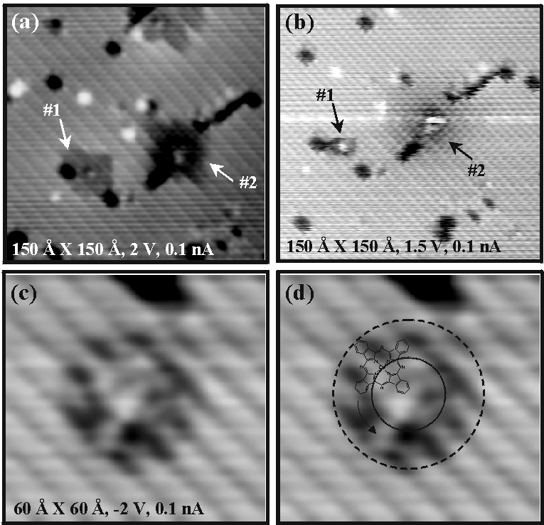 |
| Figure 5. (a) STM image (2 V, 0.1 nA) of CuPc molecules isolated using the FCL technique. Molecule #1 possesses four-fold symmetry, whereas molecule #2 possesses radial symmetry. (b) Another image of molecules #1 and #2 at a reduced bias of 1.5 V. Molecule #1 exhibits the expected 16 Å diameter, whereas molecule #2 perturbs the surface over a diameter of ~35 Å. (c) Filled states STM image of an isolated NH3-reacted CuPc molecule. (d) Overlaid on the image from part (c) is a schematic of a CuPc molecule (drawn to scale) anchored to a dangling bond via one of its outer benzene rings. The arrow suggests that rotation about this axis would sweep out a circle with the observed diameter of ~30 Å. |
4.2. Behavior of NH3-reacted CuPc
As discussed above, CuPc exhibits two distinct binding configurations with the FCL patterned sites. In one case CuPc appears tightly bound by the central metal atom and in the other case it is less tightly bound and exhibits rotational freedom. This suggests that reducing the ability of the central Cu atom to bond with the surface should lead to a preference of the loosely bound rotational configuration. The approach taken to test this hypothesis was to expose the CuPc source to 100 L of NH3 in situ prior to sublimation onto a freshly depassivated site. From conductivity measurements on CuPc films, it has been previously determined that ammonia irreversibly reacts with CuPc at room temperature [19]. The resulting behavior of an adsorbed NH3-reacted molecule is shown in the filled states STM image in Figure 5(c). In contrast to plain CuPc, which appears bright in filled states [7], the NH3-reacted CuPc molecule predominately appears as a circular depression with a diameter of ~30 Å. In addition, the interior of the NH3-reacted CuPc molecule possesses bright features that appear to compose an inner ring. Figure 5(d) presents a qualitative explanation of this interesting behavior by superimposing a schematic (drawn to scale) of a CuPc molecule onto the STM image. If the NH3-reacted CuPc spins about an anchored benzene ring at the center of the depression, then the expected result would be a circular feature with a diameter of ~30 Å. Furthermore, the ammonia bound to the central copper atom should appear as a topographic protrusion that sweeps out a smaller circle as the molecule rotates about the anchored benzene ring. The appearance of the ~15 Å diameter bright inner ring within the 30 Å radially symmetric feature in the STM topograph is consistent with this expectation.
4.3. STM spectroscopy on CuPc
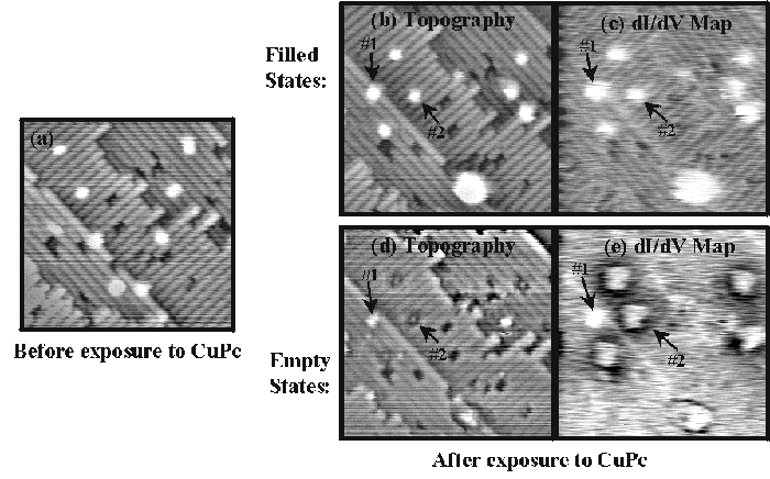
STM spectroscopy can be used to gain additional insight into the electronic and chemical structure of individual molecules isolated with FCL. This is illustrated in Figure 6 where FCL is first used to create a V-pattern of dangling bonds (Figure 6(a)) and then the surface is dosed with CuPc. Figures 6(b-e) show the results of the CuPc dose as a set of filled and empty states topographs and corresponding dI/dV images, all of which were obtained during a single scan. The dI/dV signal was measured using a lock-in amplifier with a 10 kHz 30 mV rms ac signal added to the dc tunneling bias. Several observations can be made from Figure 6. First, the initial V-shaped pattern has been disrupted, suggesting that the STM tip has induced the motion of CuPc molecules along dimer rows with a corresponding exchange of hydrogen in the opposite direction. The second observation is that in the filled states image the CuPc molecules are nearly indistinguishable from Si dangling bonds. However, in empty states (Figure 6(c)), the CuPc molecules appear as a bright central dot surrounded by a four-fold symmetric depression, similar to molecule #1 in Figure 5(b). Further distinctive character is exhibited by CuPc in the empty states conductance map shown in Figure 6(e). Here it is seen that each CuPc molecule is surrounded by a ring of decreased density of states for a distance of about 15 Å beyond the extent of the molecule, in strong contrast with the Si dangling bond (site #1) which remains unchanged from its filled states behavior. The depleted density of states surrounding the CuPc molecule in the conductance map suggests that charge transfer has occurred between the molecule and the adjacent surface. Since the central Cu atom is expected to change its oxidation state upon reaction with the Si dangling bond, charge transfer with the surrounding surface is expected.
larger image |
| Figure 6. (a) V-shaped pattern of eight depassivated sites created with the FCL technique under writing conditions of 2.75 V and 2 nA. The image size in all parts of this figure is 170 Å X 170 Å. Following exposure to CuPc, topographic and tunneling conductance images were obtained in filled states (b-c) and empty states (d-e). In empty states topography and dI/dV images, a clear distinction can be observed between an isolated dangling bond (labeled #1) and a CuPc molecule (labeled #2). |
As shown in Figure 6, the STM tip can induce the exchange of CuPc molecules and hydrogen atoms on adjacent dimers, thus leading to motion of CuPc along dimer rows. Rarely, the STM tip can even remove CuPc from the surface, leaving behind a silicon dangling bond. Although the ability to manipulate CuPc with the STM provides another level of nanoscale control, less perturbative imaging conditions (e.g., reduced tunneling current) can reduce the probability of disruption when minimal perturbation is desired.
5. Intramolecular electronic structure of C60
Figure 7(a) represents a constant current STM topograph of a C60 molecule and a cluster of silicon dangling bonds on a predominately H-passivated Si(100) surface. This situation was created by first depositing C60 onto a FCL binding site at room temperature. Following C60 isolation, the cluster of dangling bonds was then patterned to allow for topographical and spectroscopic comparison between clean silicon and C60. Topographically, ordered intramolecular structure is clearly observed for C60. The image is reminiscent of previous work and represents the spatial distribution of the occupied molecular orbitals at this energy [11-13]. For spectroscopic measurements, the tunneling conductance was measured using a lock-in amplifier when the sample bias was modulated with a 20 kHz, 120 mV rms signal. To gain both energetic and spatial dependence of the LDOS, dI/dV spectra were measured at every pixel of the image for all energies in the range ± 2 eV.
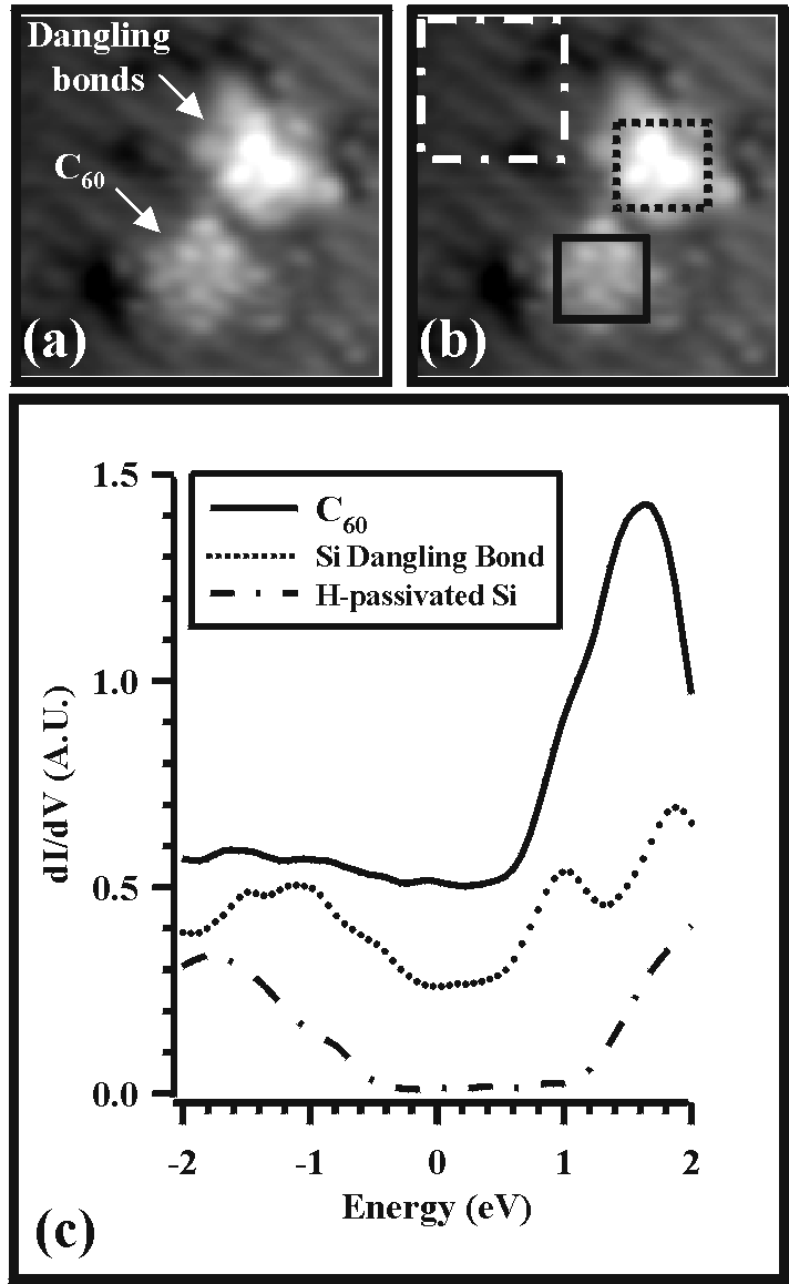 |
| Figure 7. (a) STM image (-2 V, 0.1 nA) of an isolated C60 molecule and a cluster of Si dangling bonds. (b) STM spectroscopy was performed at every pixel within this image. The spectroscopic data for all of the pixels within each box was averaged to generate the three dI/dV curves of part (c). In this paper, zero energy represents the fermi level, negative energy represents filled states (valence band), and positive energy represents empty states (conduction band). |
Figure 7(c) depicts the spatial average of the spectroscopic information for all pixels within the three labeled boxes of Figure 7(b). The spectrum for H-passivated Si possesses a relatively featureless energy gap with the fermi level positioned near the valence band, which is expected for the p-type (B-doped, 0.1 W-cm) Si sample used in this experiment. The cluster of dangling bonds exhibits richer spectroscopic structure. In particular, the energy gap is reduced, and a clear peak is visible at 1 eV. Additionally, discontinuities in dI/dV are observed at -0.5 eV and -1 eV. These three features have been calculated for the clean Si(100) surface [20] and lend credence to the validity of this spectroscopic data set. The most prevailing feature of the C60 spectrum is a strong peak at about 1.6 eV. This peak most likely represents the lowest unoccupied molecular orbital (LUMO) of the molecule. In previous work [13], researchers have observed that unoccupied states imaging is more sensitive than filled states imaging for C60 deposited on silicon at room temperature. The dominant LUMO peak in the LDOS appears consistent with this observation. Although different spectra have been previously reported for individual C60 molecules on Si(100), that data is not applicable in this case because the sample was annealed at 600°C following C60 deposition in that study [10]. This annealing step is believed to induce a transformation from physisorption to chemisorption, which would affect the LDOS [9]. In this work, C60 is often moved along or detached from the surface during imaging, which has been previously observed for the physisorbed situation [9, 12].
The clear position of the LUMO at 1.6 eV suggests the position of the highest occupied molecular orbital (HOMO). Theoretically, the HOMO-LUMO transition energy has been calculated to be 1.9 eV for free C60 molecules [21]. Similarly, experiments on free C60 molecules in solution have found the optical absorption edge to be located between 1.55 eV and 2.3 eV [22]. Assuming that the theoretical value is approximately correct, the HOMO is located about 0.3 eV below the fermi level in this case.
Figure 8 illustrates three dI/dV curves spatially averaged within three distinct areas of the C60 molecule. Spectrum b is averaged over the binding site between the C60 molecule and the underlying silicon dangling bond. As expected, this intramolecular location is most sensitive to the substrate as evidenced by the appearance of a feature at 1 eV that coincides well with the 1 eV peak in the clean silicon spectrum. The right side of the C60 molecule clearly shows the LUMO at the dominant position of 1.6 eV, whereas the left side of the molecule exhibits an apparent shift in the LUMO to ~0.7 eV. Although the cause of this shift is still under investigation, the three dI/dV curves demonstrate the ability of this experimental technique to detect intramolecular electronic structure.
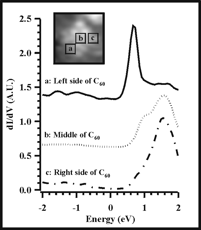 |
| Figure 8. Intramolecular spectroscopic structure is depicted by averaging the dI/dV data within three separate regions of the C60 molecule. The left side, middle, and right side of the molecule are labeled with boxes overlaid on the STM image (see inset). |
6. Conclusions
Individual organic molecules have been isolated and characterized with the STM. With FCL, arrays of dangling bonds can be reliably patterned on the Si(100)-2X1:H surface with atomic precision. Since these dangling bonds serve as effective binding sites, molecules delivered to the surface in the gas phase self-assemble into the predefined patterns. The flexibility of this self-assembly technique has been demonstrated for three separate molecules: NBE, CuPc, and C60. Following molecular isolation, STM analysis has been performed via constant current topography images and tunneling conductance imaging. In topographic images, intramolecular structure and molecular rotation have been observed for CuPc. Additionally, charge transfer from the substrate to the CuPc molecule has been detected in empty states tunneling conductance maps. For C60, the LUMO is clearly resolved in LDOS data, and intramolecular electronic structure is observed by spatially and energetically resolved tunneling conductance data. Overall, the wealth of molecular scale information generated by these initial experiments suggests the utility of this experimental technique for empirically screening molecules for various applications. The integration of FCL with an appropriately chosen molecule and a macroscopic electrical interface [23] opens many possibilities for molecular electronic device fabrication on the Si(100) surface.
Acknowledgments
The authors have benefited from discussions with Prof. Karl Hess, Prof. Jeffrey Moore, Dr. Hyungsoo Choi, Dr. Blair Tuttle, Scott Thompson, Neil Viernes, Vance Wong, and Ryan Pearman. M. C. Hersam thanks the National Science Foundation for a Graduate Research Fellowship (1997-1999) and the IBM Corporation for a Distinguished Graduate Fellowship (1999-2000). This work was supported by the Office of Naval Research Multidisciplinary University Research Initiative (MURI) under grant number N00014-98-I-0604.
References
- Reed M. A., 1999, "Molecular-scale electronics," Proceedings of the IEEE, 87, 652.
- Seabaugh A. C. and Mazumder P., 1999, "Scanning the issue," Proceedings of the IEEE, 87, 535.
- Lyding J. W., Shen T.-C., Hubacek J. S., Tucker J. R. and Abeln G. C., 1994, "Nanoscale patterning and oxidation of H-passivated Si(100)-2x1 surfaces with an ultrahigh vacuum scanning tunneling microscope," Appl. Phys. Lett., 64, 2010.
- Abeln G. C., Hersam M. C., Thompson D. S., Hwang S.-T., Choi H., Moore J. S. and Lyding J. W., 1998, "Approaches to nanofabrication on Si(100) surfaces: selective area chemical vapor deposition of metals and selective chemisorption of organic molecules," J. Vac. Sci. Technol., B16, 3874.
- Abeln G. C., Lee S. Y., Thompson D. S., Moore J. S. and Lyding J. W., 1997, "Nanopatterning organic monolayers on Si(100) by selective chemisorption of norbornadiene," Appl. Phys. Lett., 70, 2747.
- Lippel P. H., Wilson R. J., Miller M. D., Wöll Ch. and Chiang S., 1989, "High-resolution imaging of copper-phthalocyanine by scanning-tunneling microscopy," Phys. Rev. Lett., 62, 171.
- Kanai M., Kawai T., Motai K., Wang X. D., Hashizume T. and Sakura T., 1995, "Scanning tunneling microscopy observation of copper-phthalocyanine molecules on Si(100) and Si(111) surfaces," Surf. Sci., 329, L619.
- Hashizume T. and Sakurai T., 1994, C60 adsorption on the Si(100)2X1 and Cu(111)1X1 surfaces," J. Vac. Sci. Technol., B12, 1992.
- Chen D. and Sarid D., 1995, "An STM study of C60 adsorption on Si(100)-(2X1) surfaces: from physisorption to chemisorption," Surf. Sci., 329, 206.
- Yao X., Ruskell T. G., Workman R. K., Sarid D. and Chen D., 1996, "Scanning tunneling microscopy and spectroscopy of individual C60 molecules on Si(100)-(2X1) surfaces," Surf. Sci., 366, L743.
- Yao X., Ruskell T. G., Workman R. K., Sarid D. and Chen D., 1996, "Intramolecular features of individual C60 molecules on Si(100) observed by STM," Surf. Sci., 367, L85.
- Moriarty P., Ma Y. R., Upward M. D. and Beton P. H., 1998, "Translation, rotation and removal of C60 on Si(100)-2X1 using anisotropic molecular manipulation," Surf. Sci., 407, 27.
- Hou J. G., Jinlong Y., Haiqian W., Qunxiang L., Changgan Z., Hai L., Wang B., Chen D. M. and Qingshi Z., 1999, "Identifying molecular orientation of individual C60 on a Si(111)-(7X7) surface," Phys. Rev. Lett., 83, 3001.
- Gimzewski J. K. and Joachim C., 1999, "Nanoscale science of single molecules using local probes," Science, 283, 1683.
- Horn K. M., Swartzentruber B. S., Osbourn G. C., Bouchard A. and Bartholomew J. W., 1998, "Electronic structure classifications using scanning tunneling microscopy conductance imaging," J. Appl. Phys., 84, 2487.
- Stipe B. C., Rezaei M. A. and Ho W., 1998, "Single-molecule vibrational spectroscopy and microscopy," Science, 280, 1732.
- Gimzewski J. K., Joachim C., Schlitter R. R., Langlais V., Tang H. and Johannsen I., 1998, "Rotation of a single molecule within a supramolecular bearing," Science, 281, 531.
- Andersohn L. and Köhler U., 1993, "In situ observation of water adsorption on Si(100) with scanning tunneling microscopy," Surf. Sci., 284, 77.
- Kaufhold J. and Hauffe K., 1965, "Über das leitfähigkeitsverhalten verschiedener phthalocyanine im vacuum und unter dem einfluß von gasen," Ber. Bunsenges. Phys. Chem., 69, 168.
- Pollman J., Krüger P. and Mazur A., 1987, "Self-consistent electronic structure of semi-infinite Si(001) (2X1) and Ge(001) (2X1) with model calculations for scanning tunneling microscopy," J. Vac. Sci. Technol., B5, 945.
- Saito S. and Oshiyama A., 1991, "Cohesive mechanism and energy bands of solid C60," Phys. Rev. Lett., 66, 2637.
- Dresselhaus M. S., Dresselhaus G. and Eklund P. C., 1996, Science of Fullerenes and Carbon Nanotubes (San Diego: Academic Press), p. 63.
- Hersam M. C., Abeln G. C. and Lyding J. W., 1999, "An approach for efficiently locating and electrically contacting nanostructures fabricated via UHV-STM lithography on Si(100)," Microelectronic Engineering, 47, 235.
|